Products
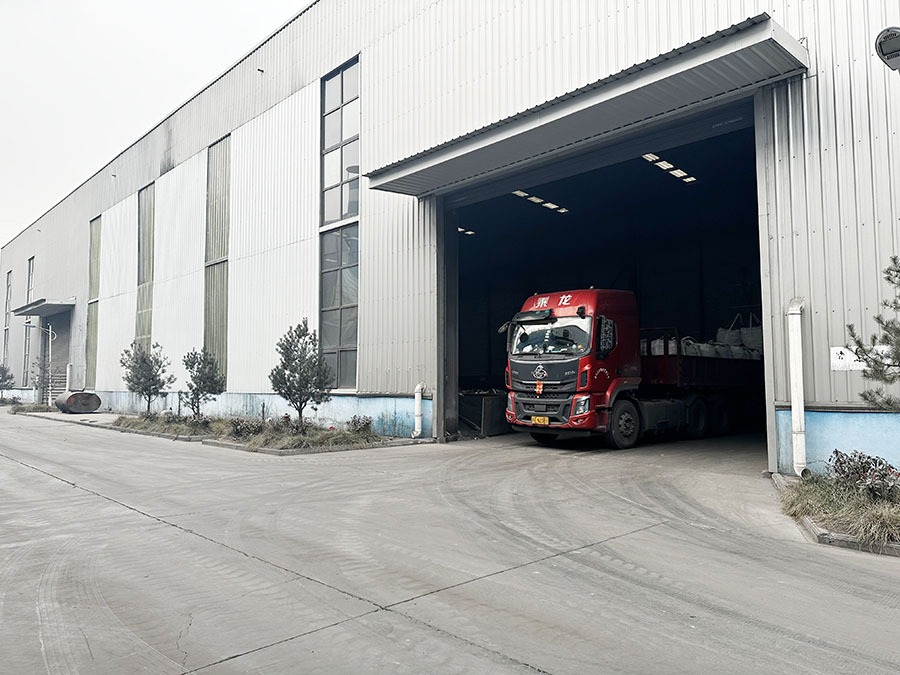
The company's products are exported to many countries, such as Japan, Turkey, India, Europe, etc., with their excellent quality performance and high-quality after-sales service, and are deeply trusted and praised by customers.

Anyang Junfa Metallurgical Materials Co., Ltd.
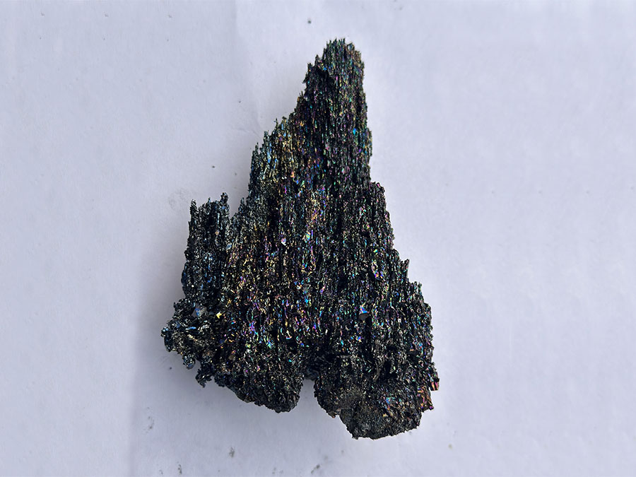
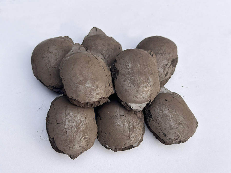
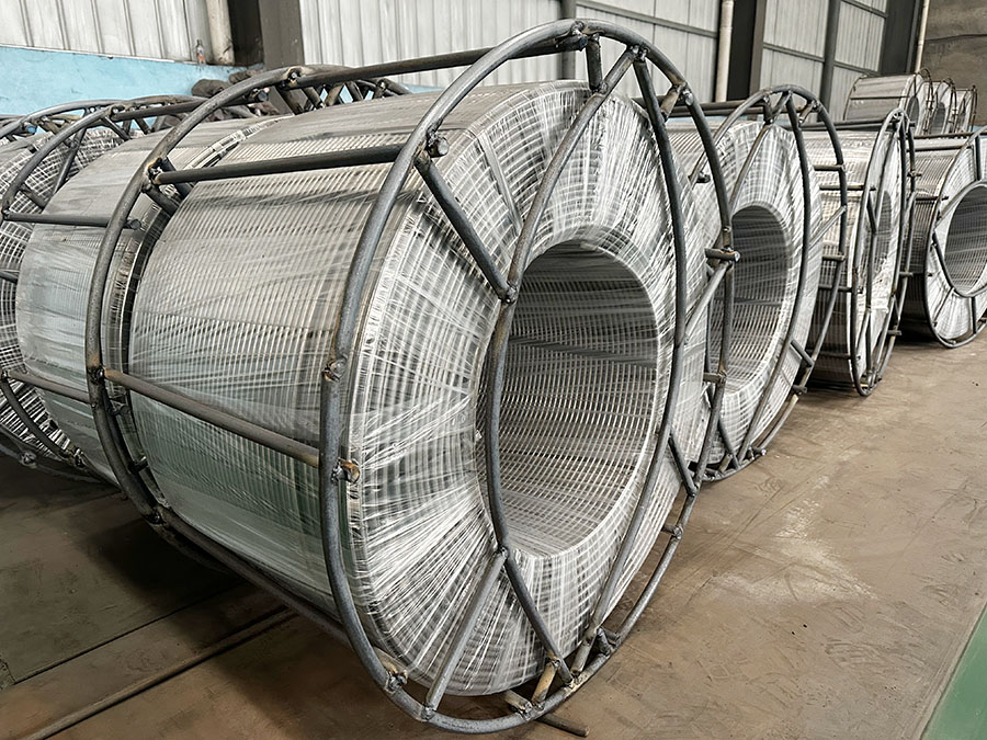
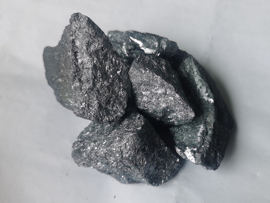
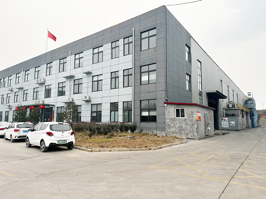
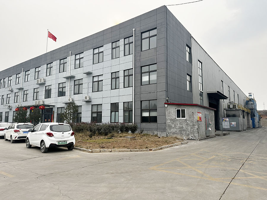
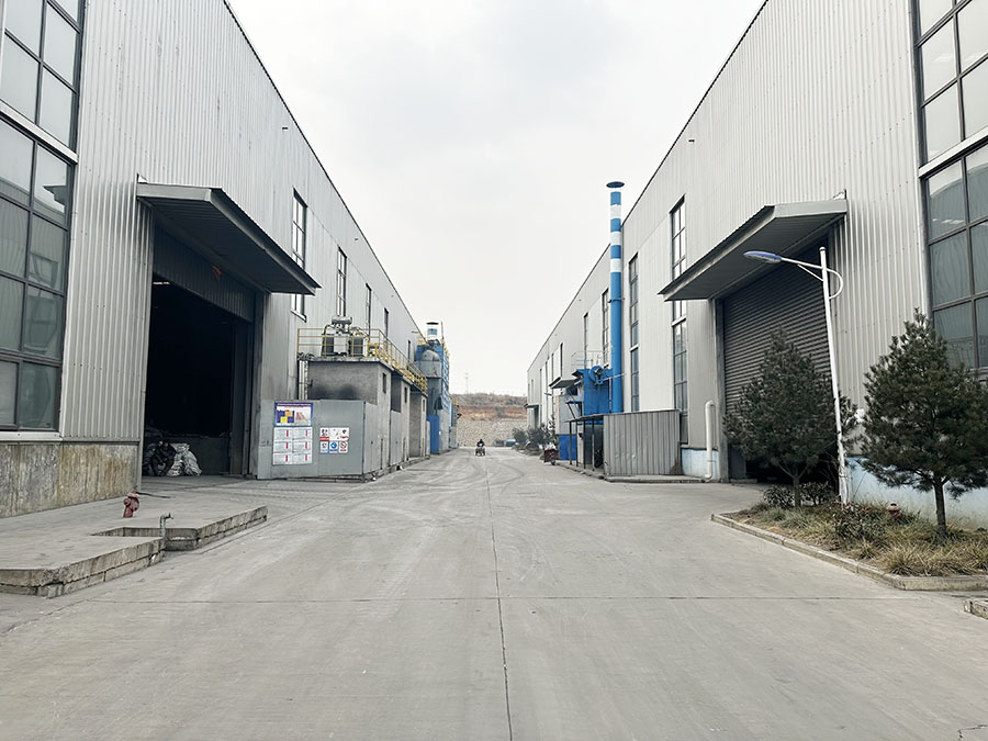
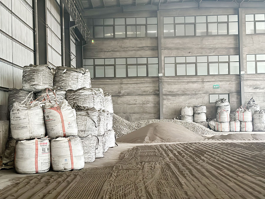
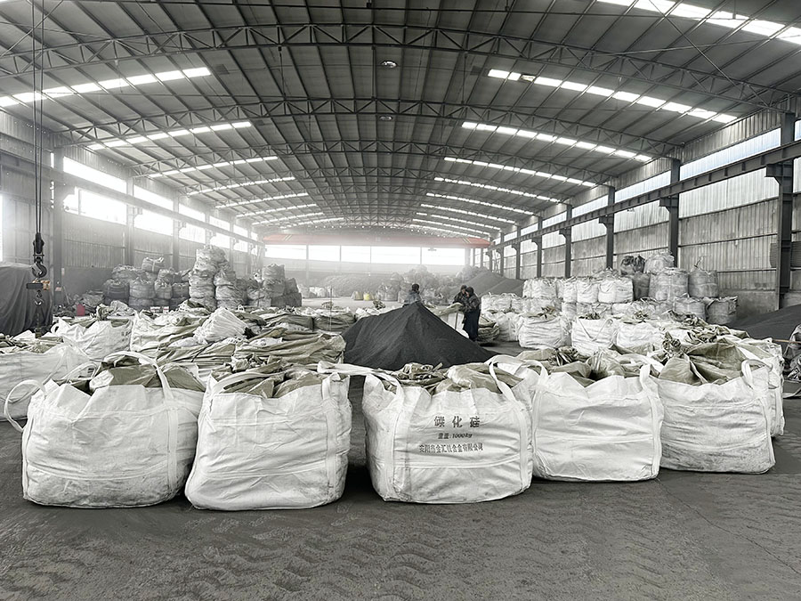
Anyang Junfa Metallurgical Materials Co., Ltd. is located in Anyang City, Henan Province. It is a modern enterprise specializing in the processing and sales of metallurgical refractory materials. Its main products include metal silicon, silicon carbide, ferrosilicon, low-silicon iron powder, silicon-calcium alloy, alloy balls, alloy cored wires and other metallurgical refractory products of various specifications and models. With the business policy of "honest management, mutual benefit", the company has developed into a well-known enterprise in the same industry. The company has fo...
CONTACT:
Address: UNIT 1406B,14/F, THE BELGIAN BANK BUILDING, NOS.721-725 NATHAN ROAD, KOWLOON, HONGKONG
Phone: +86 16692266789
Email: wyl@jfalloy.com
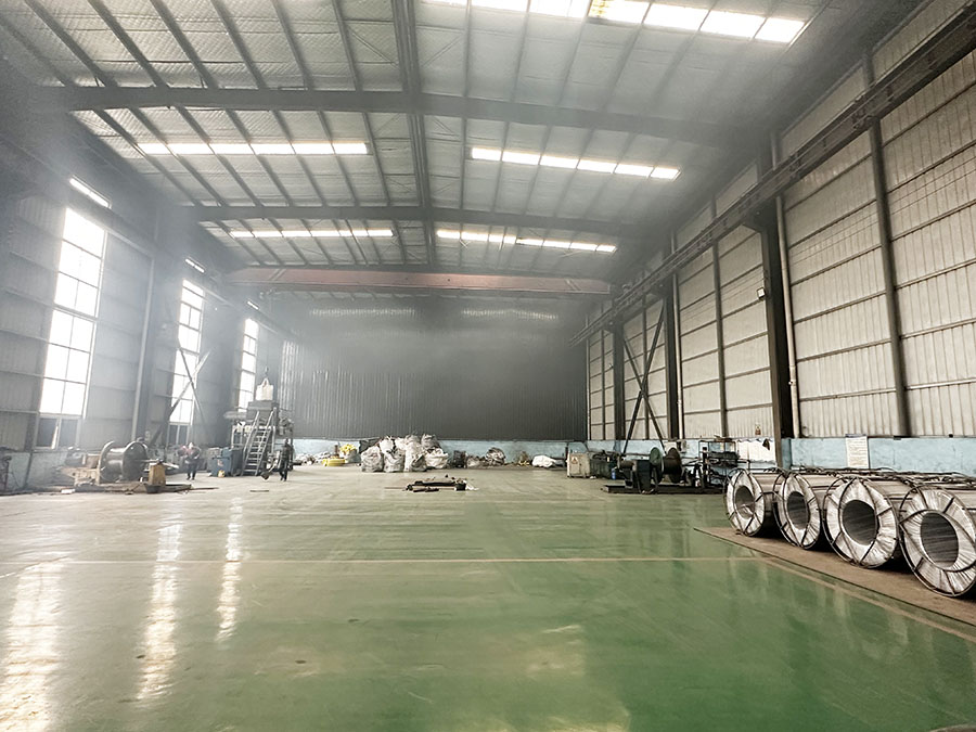
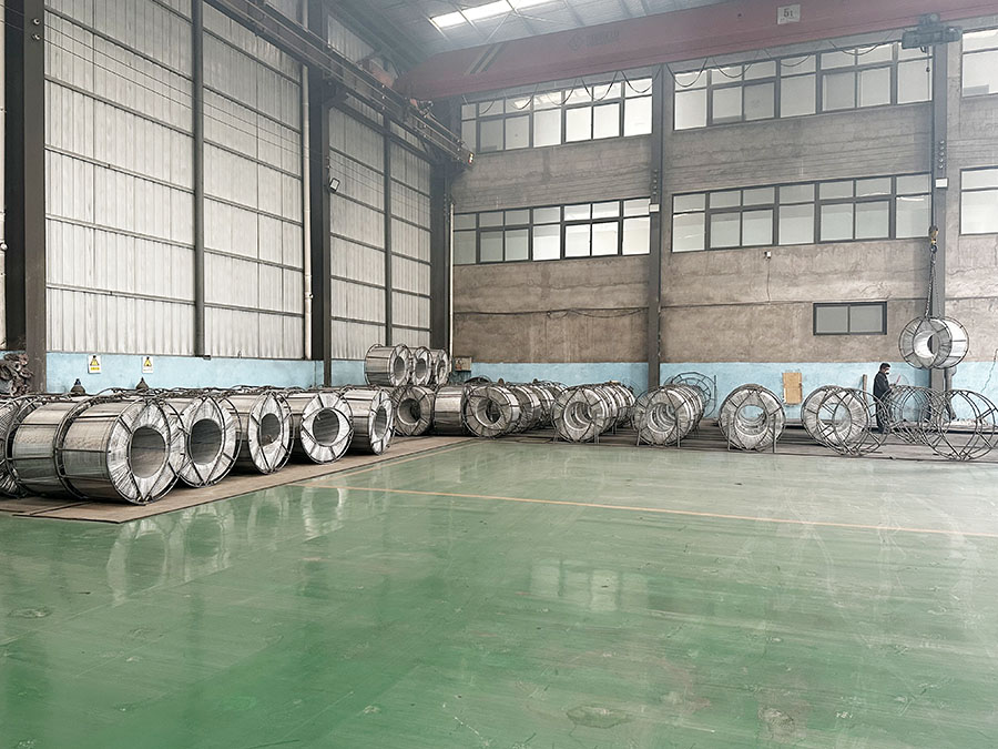
Factory AlbumMore +
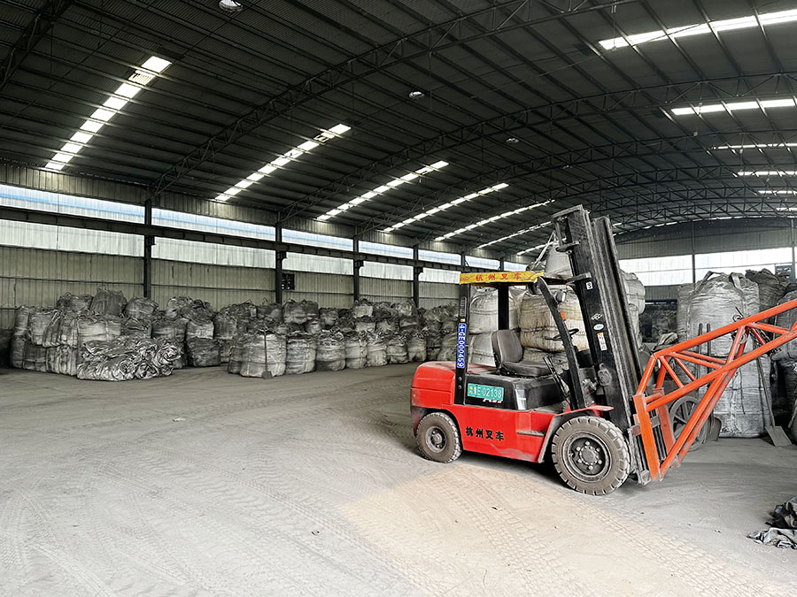
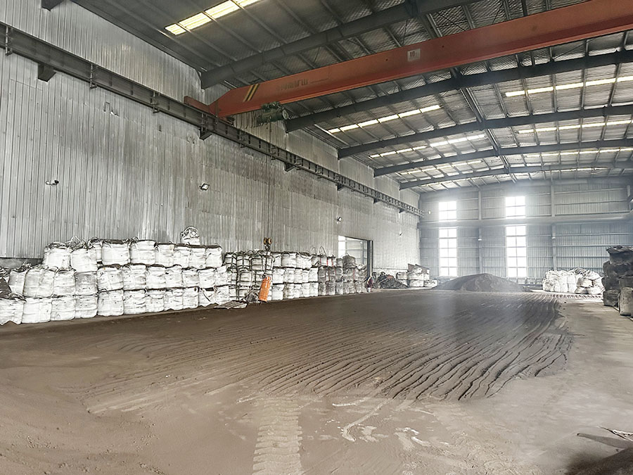
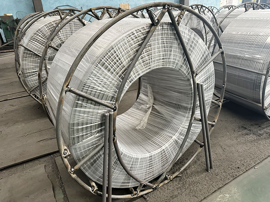
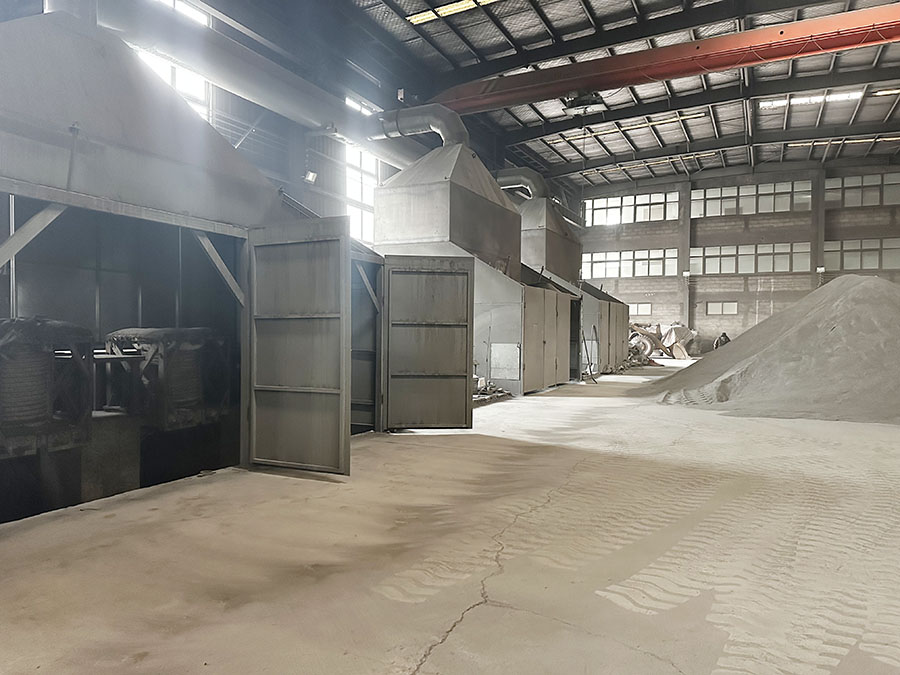
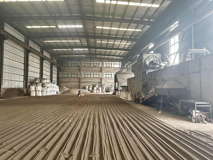
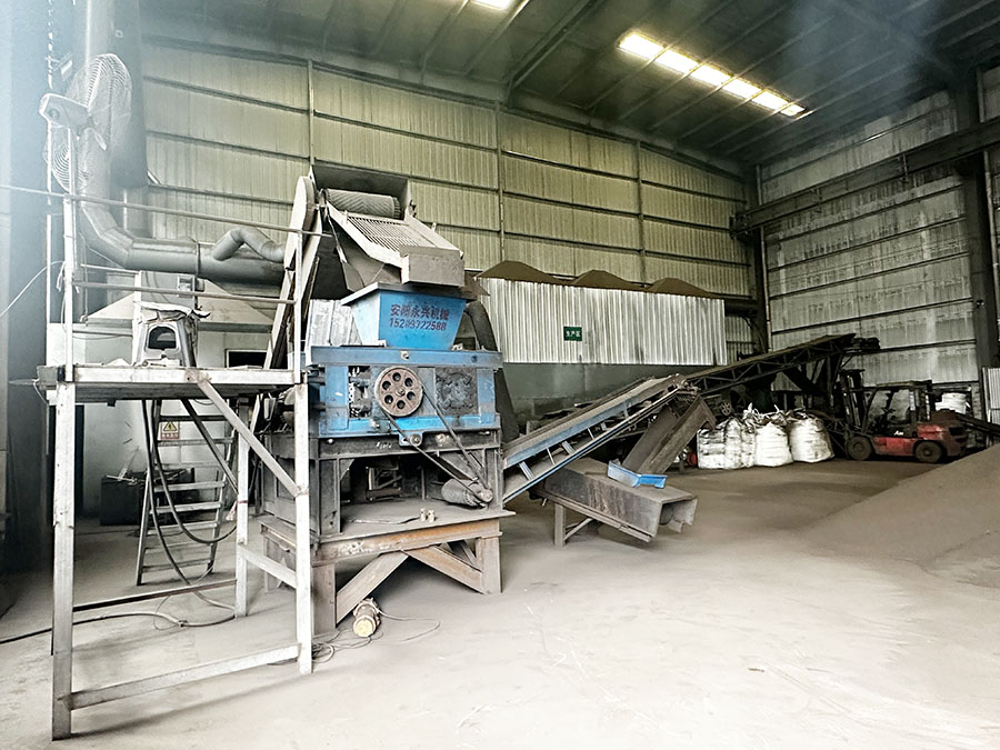
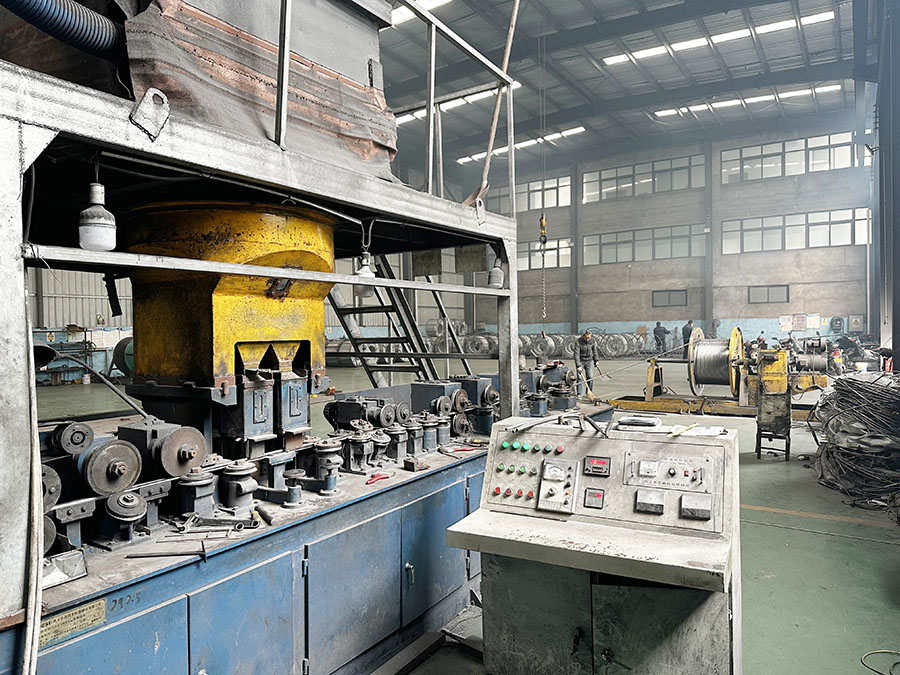
The company has four medium-frequency electric furnaces, two cored wire production lines, one ball press and one dryer, realizing high-quality, high-yield, low-consumption advanced production technology.

News
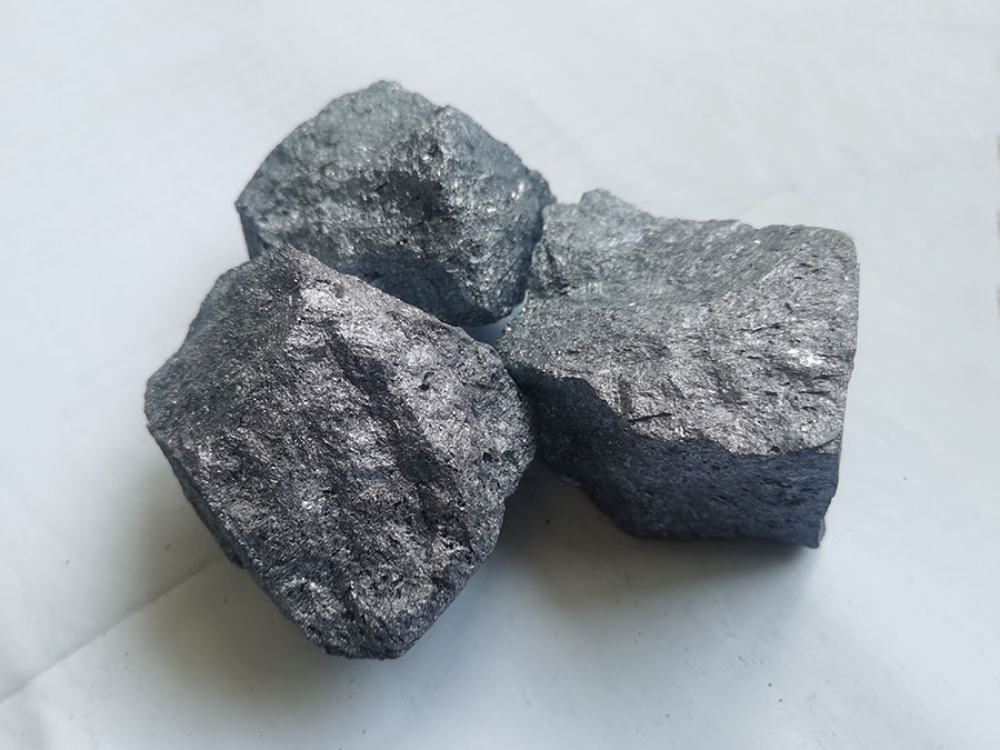
Our main products include metal silicon, silicon carbide, ferrosilicon, low-silicon iron powder, silicon-calcium alloy, alloy balls, alloy cored wires and other metallurgical refractory products of various specifications and models.